Deep learning-based detection of defects in wafer buffer zone during semiconductor packaging process
- Journal
- Multiscale Science and Engineering
- Volume
- 6
- Page
- 25-32
- Year
- 2024
- Date
- 2024-03-01
Abstract
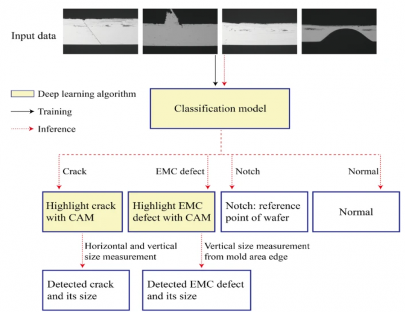
Effectively detecting defects in wafer buffer zones is crucial in semiconductor manufacturing processes. If defects are not detected in the middle of the semiconductor manufacturing process, the semiconductor eventually becomes a defective product after all processes are completed. To solve this problem, rule-based vision algorithms have been used to identify defects in the wafer buffer zone. After photographing the wafer buffer zone using a high-speed camera, defects are detected using the pixel values of the images. However, because of the resin bleed in the wafer, which is an epoxy compound, it is difficult to detect defects. Therefore, we introduced a deep learning method for semiconductor inspection and created a high-performance semiconductor inspection algorithm. The defects in the wafer buffer zone should be detected accurately and quickly. Furthermore, the approximate size of the defects must be extracted. We modified the Xception model to fit the wafer data characteristics considering both accuracy and speed. We proposed to extract the size of the defect using class activation mapping (CAM). We obtained an accuracy of 96.9% from the actual wafer dataset through this framework, and then managed to extract the size of the defect through CAM.

